


Tevet Process Controls Wins Editor's Choice Award
Tevet Process Controls Wins Editor's Choice Award
Semiconductor International Magazine Recognizes Flagship Product
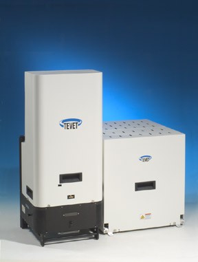
Tevet Process Control Technologies, at 5673 W. Las Positas, Boulevard, was honored in July with an Editors' Choice Best Product Award by industry journal Semiconductor International for its Trajectory T3 metrology module. The Trajectory T3 is a tool used to achieve the exacting measurements necessary in the production of semiconductors with minimal waste of raw materials. Semiconductors are the "chips" used in products that include the processors in computers. According to the magazine: "The chosen products were recognized for their proven excellence in the advancement of wafer processing, chip assembly or packaging, and process testing capabilities..." The extent to which the products improved employee productivity, among other criteria, was also considered in choosing winners of the awards.
Tevet's Trajectory T3 is used by semiconductor manufacturers to measure the materials deposited on silicon wafers. During the production of semiconductors, machinery places materials in layers on the silicon base material. These materials include multiple layers of circuitry that carry electrical currents (akin to the wiring on multiple floors of a building), and what are known in the industry as "thin films," which separate and insulate these lines of circuitry. These films deposited between and underneath the microscopic "wires" of circuitry are every bit as important as the circuits themselves, acting as insulation to ensure that the electrical currents flow as planned.
Before the development of tools like Tevet's system, obtaining the correct thickness of circuits and film was primarily a trial-and-error process. Manufacturers would perform a test run to measure these materials and, if they were within the right specifications, production would continue. If they were not correct, manufacturers would have to figure out what the problem was and try again. In the process of fine tuning the processing procedure, large amounts of material were often wasted.
Tevet's system uses an integrated sensor that is attached to a silicon wafer production machine to automatically measure the thickness of materials deposited on every silicon wafer without interfering with the production process. The result is that manufacturers waste fewer raw materials in ensuring that semiconductors are made correctly. Because the Trajectory T3 module is added to existing production line machinery rather than requiring that manufacturers retool all of their processes, it is considered a cost effective solution when compared to the waste associated with other methods of measurement.
"Our Trajectory T3 was considered for the award along with products in and outside of our market segment," says Peter Gillespie, Tevet's vice president of marketing and sales. "Hundreds of products are eligible for the award and, this year, we were one of the small group of entrants that won." Tevet's system has been adopted by multiple customers in Europe, Israel, Asia, and the U.S. and recently achieved sales of 10 and 15 units respectively at each of two semiconductor fabrication sites. Typically, each site only purchases one or two of the systems, making these sales achievements noteworthy.
Tevet Process Control Technologies was established in 1999 in Israel. The company's facility in Hacienda, which opened in January 2003, serves as Tevet's U.S. headquarters, providing marketing, sales, applications engineering, and customer support for its customers around the world. The company's research and development takes place at its headquarters in Yoknea'm, Israel and its offices in Hacienda are responsible for sales, marketing, and technical support. Tevet has five employees in Pleasanton and 25 worldwide.
"We've created a new model for integrated measurement in the semiconductor industry," Gillespie says. "We have now achieved the first critical adoption of our systems as well as placements with a number of key customers. This award recognizes that we're on the right path in this new product area. We're going through a profound growth stage right now and it's an exciting time for us."
Also in this issue...
- Kaiser Permanente Purchases Four Buildings in Hacienda
- Tevet Process Controls Wins Editor's Choice Award
- Business Bits
- Executive Profile: Erin Kincheloe, Cents & Sensibility, Inc.
- Kohzu America Moves Devices with Precision
- No matter the Asset, Allstate Insurance Keeps Customers Covered
- 511 is the Answer to Your Bay Area Transit and Travel Questions
- Join the Great Race for Clean Air and You Could Win a Trip to Santa Barbara
- City of Pleasanton Seeks Business Partners for LEAP Program
- Child Care Links Seeks Entrants for "Family Friendly Employer of the Year" Contest
- Circus Chimera
- Hacienda Index
- Calendar