


Tevet Process Control Technologies Opens Facility in Park
Tevet Process Control Technologies Opens Facility in Park
New Offices Will House Company's Business Operations to Support R&D in Israel
Tevet Process Control Technologies, a start up company that builds specialized manufacturing tools for the semiconductor industry, recently leased offices at 5673 W. Las Positas Boulevard, Suite 213 in the Stoneridge Business Center. The new facility will serve as Tevet's U.S. headquarters, providing marketing, sales, applications engineering, and customer support for its customers around the world.
Tevet Process Control Technologies was established in 1999 in Israel. The founders of the company all came from the semiconductor industry with extensive knowledge and experience in semiconductor process technology. "The top four or five people in the company all together have over a hundred years of experience in semiconductor processing and technology," says Yuval Wasserman, President of Tevet Process Control Technologies. "The idea behind the company came from the fact that the founders realized that process control in the semiconductor industry was not very automatic. It was very 'human dependent' and a lot of engineering time was spent running tests to qualify the machines for mass production."
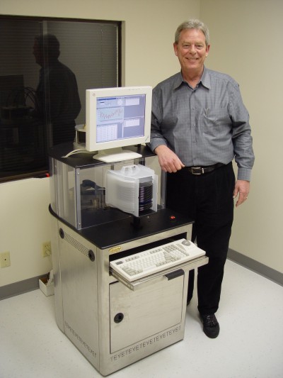
Tevet's In-Situ Thickness Measurement System ensures that the films deposited on silicon wafers-like those used to make such products as the main processors for computers-had the right thickness. Traditionally, to make sure that the wafers were being produced correctly, the manufacturers would occasionally do a test run and measure the thickness of the film on the wafers. If the thickness of the film was within the right specifications, they would keep running production. If it was not correct, they would have to figure out what went wrong with the processing tool. In the process, semiconductor manufacturers would frequently have to waste large amounts of silicon when they finally discovered a problem, throwing out the material that was manufactured preceding the time they found a problem.
Tevet's system involves using an integrated sensor that is hooked onto a silicon wafer production machine to automatically measure the thickness of the thin films deposited on every product wafer without interfering in the production process. In effect, it attaches to existing microprocessor production tools to keep the manufacturers from wasting materials and to ensure that the chips are made correctly.
"We have our business operation in the Bay Area to shorten the distance between us and our customers," Wasserman says. "We sell in Asia, in Europe, and in the U.S. Our location in Israel is very attractive for research and development and the Bay Area is very important in promoting our business. We found dealing with the Business Center here very pleasant. We enjoy the services here and the surroundings. It's very conducive for start up high-tech companies."
Tevet currently has its measurement system installed in three "beta" test sites-one of them with an equipment manufacturer and two in semiconductor fabrication facilities. The company's exuberance brings back images of the glory days of high tech startups. "We're having a lot of fun," Wasserman says. "Starting with an idea, taking technology that was proven in a lab, developing it, and making a business out of is exciting."
Photo: Ralph Mason, Tevet's global sales manager, stands with one of the company's products.
Also in this issue...
- Option One Mortgage Corp. Opens Doors at Hacienda
- P3 Party Place Offers Parents Childcare on an As-Needed Basis
- Business Bits
- Executive Profile: Glen Martin, Standard Pacific Homes
- Modius Merges IT and Device Management
- Paramount Pest Control Keeps Unwanted Visitors Out of Homes and Businesses
- www.Hacienda.org: Your Source for Information on Hacienda and the Tri-Valley
- Growing Pleasanton Non-Profit Provides Blankets for Kids
- Alameda County Fairgrounds Offers Facilities for Large Events, Conferences, with an Eye Towards Possible Expansion
- Tri-Valley Regional Mixer Offers One-Stop Shopping for Business Community
- Donations Sought for 2004 Hacienda Food Drive
- Hacienda Index
- Calendar